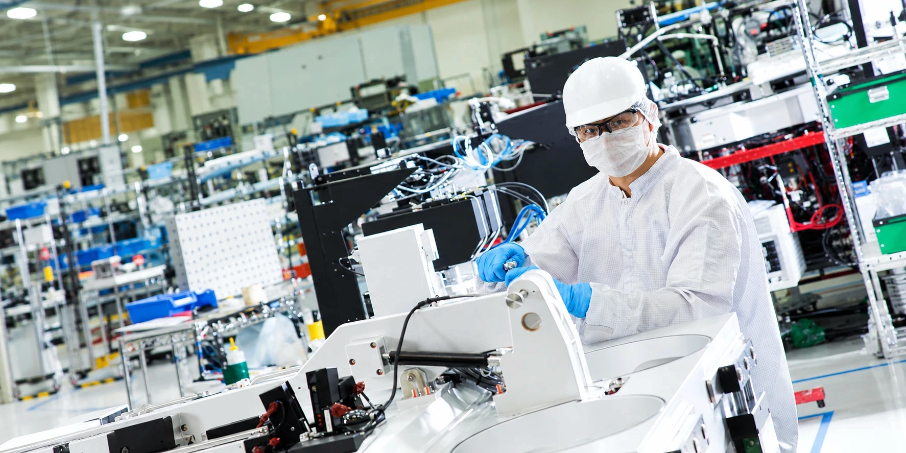

Engineer assembling semiconductor equipment in a cleanroom

Powered by

Connect with
Applied Materials

An invite-only evening for semiconductor professionals.

4th December, Friday, 2026
5 PM Onwards

[Venue TBC] · Bay Area, California

Event begins in

52Days. 18Hours. 41Minutes. 42Seconds.

52 Days. 18 Hours. 41 Minutes. 42 Seconds.

Engineer assembling semiconductor equipment in a cleanroom

Powered by

Connect with
Applied Materials

An invite-only evening for semiconductor professionals.

4th December, Friday, 2026
5 PM Onwards

[Venue TBC] · Bay Area, California

Event begins in

52Day 18Hr 41Min 42Sec

An Exclusive Evening

More than an evening
A chance to explore what’s next.

More than an evening
A chance to explore what’s next.

More than an evening
A chance to explore what’s next.

Join us for an evening of ideas, deep-tech conversations, and meaningful connections.

Engage with our leaders to learn about opportunities shaping the future of semiconductors and discover why Applied India is emerging as a hub to solve some of the industry’s most complex challenges.

Join us for an evening of ideas, deep-tech conversations, and meaningful connections.

Engage with our leaders to learn about opportunities shaping the future of semiconductors and discover why Applied India is emerging as a hub to solve some of the industry’s most complex challenges.

Join us for an evening of ideas, deep-tech conversations, and meaningful connections.

Engage with our leaders to learn about opportunities shaping the future of semiconductors and discover why Applied India is emerging as a hub to solve some of the industry’s most complex challenges.

  • Applied Materials leaders with guests at the SEMICON India booth
  • Applied Materials India leaders in a panel discussion on India’s semiconductor ecosystem
  • Applied Materials leaders networking with guests
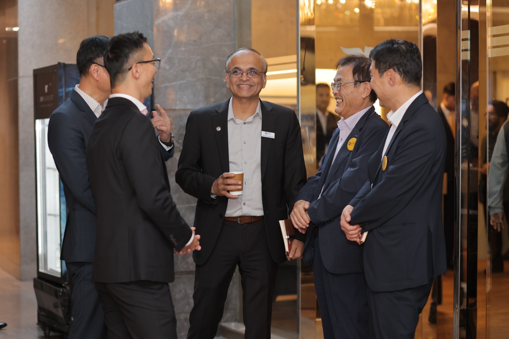
  • Applied Materials leaders in conversation at an industry evening

Who should attend

Who should attend

Who should attend

Seasoned engineers and leaders from the semiconductor industry.

Seasoned engineers and leaders from the semiconductor industry.

Seasoned engineers and leaders from the semiconductor industry.

Professionals curious about contributing to India’s semiconductor and

AI ecosystem.

Professionals curious about contributing to India’s semiconductor and AI ecosystem.

Agenda

How the evening unfolds.

How the evening unfolds.

How the evening unfolds.

Hover over a session to learn more

Tap a session to learn more

Tap a session to learn more

5:00

Welcome &
Registration

5:30

Opening
Keynote

5:45

Inside Applied Materials:
Innovation

6:00

Fireside
Chat

6:45

Q&A with
Leadership

7:00

Meet Applied Materials:
Breakouts

8:00

Closing
Remarks

8:05

Networking
& Dinner

5:00–5:30 PM

01 / 08

Welcome & Registration

Effortless check-in and a warm welcome. An early opportunity to meet fellow attendees and begin conversations before the formal programme opens.

5:00–5:30 PM

Welcome & Registration

Effortless check-in and a warm welcome. An early opportunity to meet fellow attendees before the formal programme opens.

5:30–5:45 PM

Opening Keynote

A welcome address from Applied Materials leadership — setting the context for the evening and the conversations ahead.

5:45–6:00 PM

Inside Applied Materials: Innovation & Impact

A snapshot of Applied Materials’ journey, values and industry leadership — the work, the culture, and what makes the company distinct.

6:00–6:45 PM

Fireside Chat: The Future of Semicon, Tech & Talent

A candid, unscripted conversation with Applied Materials leaders on industry trends and what world-class engineering talent looks like.

6:45–7:00 PM

Q&A with Applied Materials Leadership

Open floor. Direct questions to Applied Materials leaders on culture, India, and the company’s strategic direction.

7:00–8:00 PM

Meet Applied Materials: Breakout Conversations

Small-group discussions with Applied Materials leaders — deeper dives into specific teams, projects and possibilities.

8:00–8:05 PM

Closing Remarks

A note of appreciation and next steps for those interested in continuing the conversation with Applied Materials.

8:05–9:00 PM

Networking, Cocktails & Dinner

A relaxed setting for meaningful conversations — with peers, Applied Materials leaders and the wider semiconductor community in the room.

Subject to change

Why India. Why Now?

Why India. Why Now?

Why India. Why Now?

India is emerging as one of the world’s most dynamic semiconductor ecosystems, bringing together world-class engineering talent, growing domestic demand, and strong policy support.

$100–110B

projected semiconductor market by 2030

~6%

of global semiconductor consumption

~20%

of the world’s semiconductor design talent

~$13B

government commitment through Semicon 2.0

Applied Materials India

Over two decades of innovation in India.
Building the next era of semiconductor technology here.

Over two decades of innovation in India.
Building the next era of semiconductor technology here.

Over two decades of innovation in India.
Building the next era of semiconductor technology here.

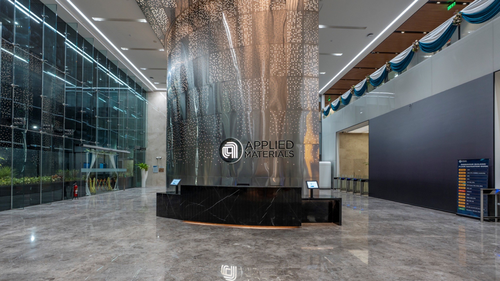
Applied Materials India office lobby
Atrium of the Applied Materials India office, Bengaluru

Our Ambition

Make in India. Invent in India. Integrate in India - for the world.

Learn more about our India journey here

01

20+ years of R&D in India, and over 750 U.S. patents granted to India employees in the last decade.

02

The India Validation Center — India’s first 300mm R&D lab, built in 2024, with Phase 2 expansion underway.

03

7,000+ employees, more than fourfold growth in a decade; 50 suppliers drove 8x year-on-year spend growth to our global factories in 2026.

04

New 8 lakh sq. ft. world-class office space in Bengaluru.

Recognition

Awards & Accolades

Awards & Accolades

Awards & Accolades

  • Zinnov Awards
  • ASSOCHAM
  • Kotler Impact
  • nasscom ER&D
  • Great Place To Work Certified, May 2026–May 2027, India
  • ET Best Tech Brands 2026

Applied India Vision

Applied Materials plans to invest $5 billion in India over the next decade - a commitment, built on three pillars.

Applied Materials plans to invest $5 billion in India over the next decade - a commitment, built on three pillars.

Applied Materials plans to invest $5 billion in India over the next decade - a commitment, built on three pillars.

01

Deepen R&D in India

‘Invented in India’

02

Accelerate the ecosystem

‘Built in India for the world’

03

Grow the future talent

‘Differentiated by talent’

Let's shape the future of semiconductor technology in India, together.

Some of the Areas Driving Growth

Process Engineering

Process Engineering

Global Product Management

Global Product Management

Technical Program Management

Technical Program Management

Systems Engineering

Systems Engineering

A look back at key moments

A look back at key moments

A look back at key moments

When we opened doors to our new office

Inauguration of the Endeavour Campus

A glimpse of Semicon India 2026

Applied Materials at SEMICON India 2026

Aerial view of Bengaluru with Vidhana Soudha and the city skyline

Life in Bengaluru

More than a technology hub. A city built for long-term living.

More than a technology hub. A city built for long-term living.

More than a technology hub. A city built for long-term living.

Bengaluru combines global career opportunities with a lifestyle that is increasingly difficult to find elsewhere. From world-class schools and healthcare to thriving cultural communities, the city offers the infrastructure and ecosystem many professionals look for when considering their next chapter.

Whether you’re raising a family, building a company, or reconnecting with India while staying close to global innovation, Bengaluru provides the balance of ambition, community, and quality of life.

Key Highlights

India’s leading technology and innovation ecosystem

International schools and healthcare facilities

Strong global professional community

Pleasant climate year-round

Modern housing and lifestyle infrastructure

Register

Some conversations are worth making time for.

Some conversations are worth making time for.

Some conversations are worth making time for.

This event is curated for relevance. Participation is by invitation, subject to profile review and capacity.

Share your profile. If your background is a strong fit, we’ll be in touch within 48 hours.

Date

4th December, Friday - 2026

04 December 2026, Friday

Time

5 PM Onwards

Location

[Venue TBC], Bay Area

Format

In-person · 3–4 hour evening

Powered by

GTX, Global Talent Exchange

Registration Request

Fill in the form below. If your background matches, you’ll hear back within 48 hours.

Your information will only be shared with Applied Materials and GTX for the purposes of this event.